As electronic products become more advanced, ensuring long-term system reliability has become a top priority. From embedded systems and industrial equipment to communication devices and consumer electronics, every component must work together efficiently to deliver consistent performance. Even a minor issue in hardware design, PCB layout, or IC packaging can affect functionality, increase maintenance costs, and delay product launches.
This is why many organizations are adopting an integrated design approach. By aligning hardware design, PCB layout, and IC packaging from the beginning of the development process, engineering teams can improve product performance, reduce design risks, and create reliable systems that meet both technical and manufacturing requirements.
What Is an Integrated Hardware, PCB Layout & IC Packaging Approach?
An integrated approach brings together multiple engineering disciplines to work as a unified team throughout product development. Instead of treating hardware design, PCB layout, and IC packaging as separate activities, these areas are planned and optimized together.
This collaborative process allows engineers to identify potential issues early, validate design decisions, and ensure every part of the system works seamlessly. It also helps reduce redesign efforts, shorten development cycles, and improve the overall quality of the final product.
Why Integration Is Essential for System Reliability
Reliable electronic systems require more than high-quality components. They depend on how effectively every element of the design works together.
Stronger Signal Integrity
As electronic devices continue to operate at higher speeds, maintaining signal quality becomes increasingly important. Poor PCB routing or hardware placement can introduce signal loss, interference, and timing issues.
An integrated design process allows engineers to optimize trace routing, grounding, impedance control, and component placement. These improvements help maintain signal integrity and ensure stable communication between components.
Effective Thermal Management
Heat can significantly impact the reliability and lifespan of electronic systems. Without proper thermal planning, excessive temperatures may reduce component performance and increase the likelihood of failure.
By considering hardware architecture, PCB layout, and IC packaging together, engineers can improve heat dissipation through optimized board layouts, thermal vias, heat sinks, and efficient airflow. Better thermal management contributes to improved reliability and consistent operation.
Stable Power Delivery
Reliable power distribution is essential for every electronic system. Voltage fluctuations or poorly designed power networks can affect overall performance and system stability.
Integrating hardware and PCB layout enables engineers to design efficient power distribution networks, optimize decoupling capacitor placement, and reduce electrical noise. This ensures stable power delivery across the entire system.
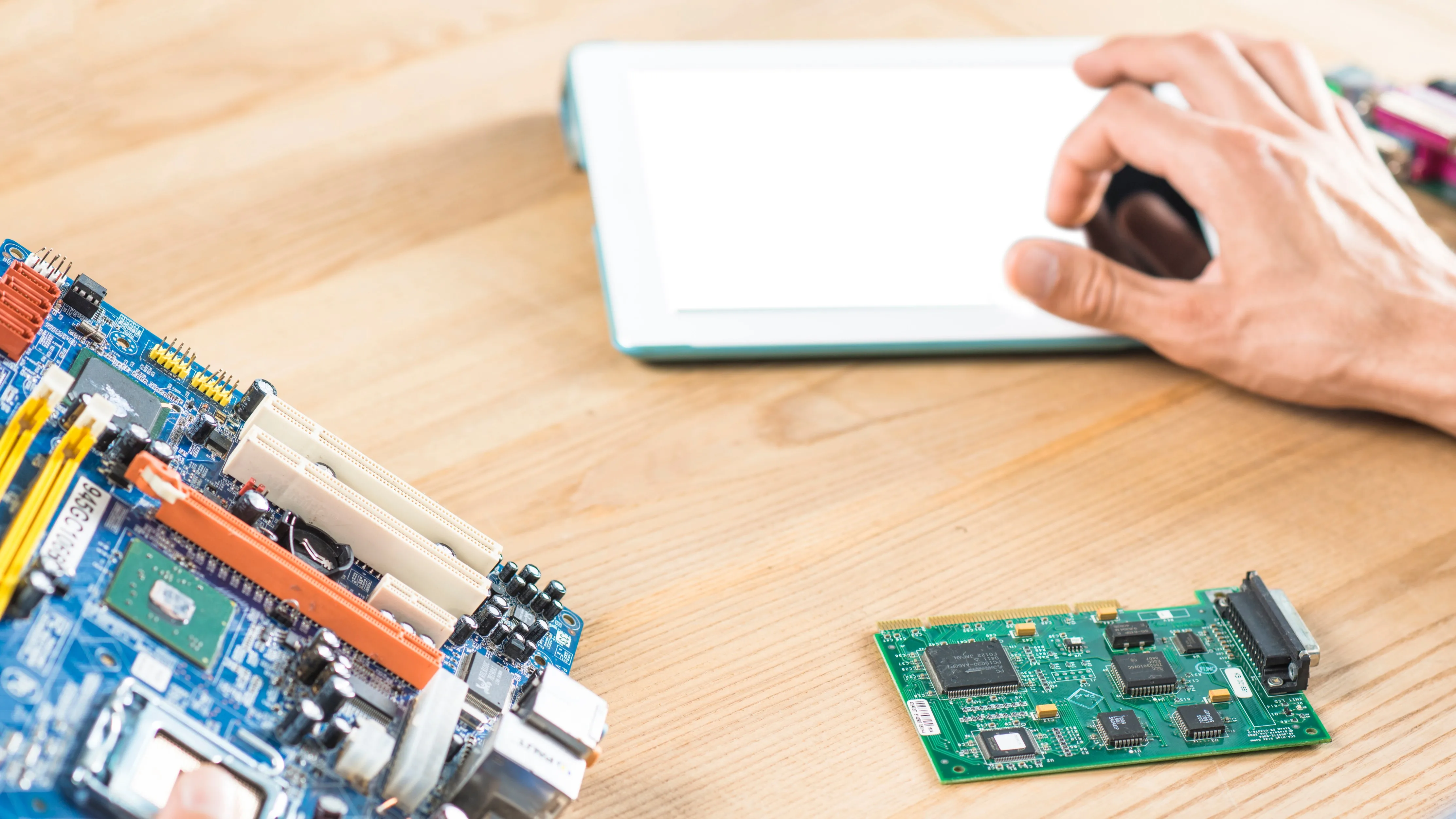
The Role of PCB Layout in Reliable Product Design
PCB layout is much more than arranging components on a board. It directly influences electrical performance, manufacturability, and long-term reliability.
A well-planned PCB layout helps achieve:
- Optimized component placement
- Controlled impedance routing
- Reduced electromagnetic interference (EMI)
- Efficient grounding strategies
- Improved thermal distribution
Better manufacturing consistency
When PCB layout is considered alongside hardware design, businesses can reduce design complexity while improving product performance and production quality.
Why IC Packaging Matters
IC packaging plays a critical role in protecting semiconductor devices while supporting electrical connectivity and thermal performance. As products become smaller and more powerful, selecting the right packaging technology becomes increasingly important.
Effective IC packaging helps:
- Improve heat dissipation
- Support high-speed signal transmission
- Increase mechanical durability
- Reduce package size
Enhance overall device reliability
When packaging decisions are aligned with hardware and PCB design, the result is a more dependable and efficient electronic system.
Benefits of an Integrated Development Strategy
Bringing hardware, PCB layout, and IC packaging together provides advantages throughout the entire product development lifecycle.
Faster Development Cycles
Early collaboration allows engineering teams to identify design challenges before prototyping or manufacturing. This reduces revisions and helps accelerate product development.
Improved Manufacturing Readiness
An integrated design process supports Design for Manufacturability (DFM), ensuring products are easier to assemble, test, and manufacture at scale. This improves production efficiency while reducing manufacturing risks.
Lower Development Costs
Resolving design issues during the early stages of development is far more cost-effective than making changes after production begins. Integrated engineering minimizes redesign efforts and helps optimize project budgets.
Greater Long-Term Reliability
Considering electrical, thermal, and mechanical requirements together creates products that perform consistently throughout their lifecycle. This reduces field failures, lowers maintenance costs, and improves customer satisfaction.
Choosing the Right Engineering Partner
Achieving reliable electronic system performance requires expertise across multiple engineering disciplines. An experienced engineering partner can help optimize every stage of development, from hardware architecture and PCB layout to IC packaging and manufacturing readiness.
At Fidus, integrated engineering teams work collaboratively to deliver solutions that balance performance, reliability, and scalability. By aligning hardware, PCB layout, and IC packaging from the start, businesses can reduce development risks and accelerate successful product delivery.
Final Thoughts
System reliability is built through careful planning, collaboration, and engineering excellence. Integrating hardware design, PCB layout, and IC packaging creates a strong foundation for developing electronic products that perform consistently under real-world conditions.
This unified approach improves signal integrity, thermal management, power distribution, and manufacturing readiness while reducing development costs and design complexity. As electronic systems continue to evolve, organizations that embrace integrated engineering practices are better positioned to deliver reliable, high-performance products that support innovation and long-term business success.